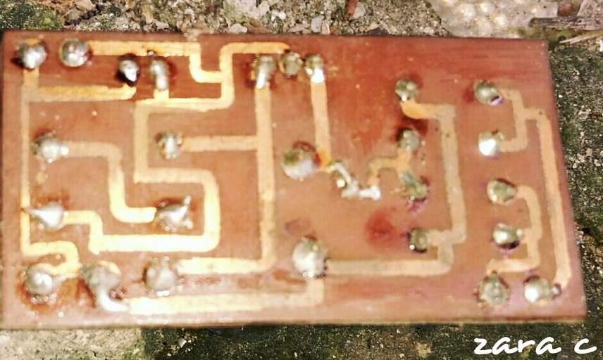
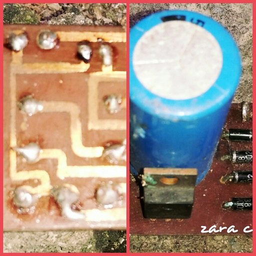
Printed Circuit Board
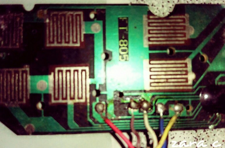
"A printed circuit board or PCB interconnects various electronics components without discrete wires. Alternative name is printed wiring board or PWB."
"The simplest PCB is a layer of copper foil glued to a sheet of plastic, often epoxy glue reinforced with fiberglass. The excess foil is removed, usually by chemical etching, and components are attached to the remaining foil, usually by soldering."
"Printed circuit technology normally uses photolithography to make the conductors. Sometimes it uses mechanical deposition to attach conductive layers to an insulating substrate. The photo mask is usually prepared with a photo plotter from data produced by a technician using computer-aided PCB design software. Some persons claim that they can produce low-resolution photo plots by printing a design to a laser printer, printing on the sheets used to make transparent presentations."
PCBs are rugged, inexpensive, and can be highly reliable. They are harder to repair than wire wrap boards. They require much more design than either wire-wrapped or point-to-point constructed equipment.
The inventor of the printed circuit was probably the Austrian engineer Paul Eisler (1907 - 1995) who, while working in England, made one in about 1936 as part of a radio set. In about 1943 the Americans began to use the technology on a large scale to make rugged radios for use in World War II. After the war, in 1948, the USA released the invention for commercial use. Printed circuits did not become commonplace in consumer electronics until the mid-1950s. Before printed circuits, point-to-point construction was used. For prototypes, or small production runs, wire wrap can be more efficient.
"Originally, every electronic component had wire leads, and the PCB had holes drilled for each wire of each component. The components were then soldered to the PCB. This method is called through-hole construction. This could be done automatically by passing the board over a ripple, or wave, of molten solder in a wave-soldering machine. Through-hole mounting is still useful in attaching physically large and heavy components to the board. However, the wires and holes are wasteful. It costs money to drill the holes, and the wires are merely cut off.
In the 1960s, a technique called surface mount was invented. It became widely used in the late 1980s. Components were mechanically redesigned to have small metal tabs or pads that could be directly soldered to the surface of the PCB. Often, only the attaching solder holds the part to the board. Surface-mount components are usually made as physically small and lightweight as possible for this reason."
Photos were taken using my mobile phone.
References
Coombs, Clye F. (1967). Printed Circuits Handbook. U.S.A.: R.R. Donnelley and Sons Company.
Crus, Roberto P. and Rogelio A. Velas (1987). Printed Arts and Home Technology in Electronics. Quezon City, Philippines: JMC Press, Inc.
Ruehli, A.E. (1987). Circuit Analysis, Simulation and Design. Vol. 3. U.S.A.: Elsevier Science Publishing Company,Inc.
No comments:
Post a Comment